MENGUATKAN INOVASI DALAM OPTIK DAN FOTONIKA MELALUI SIMULASI VIRTUAL
Telusuri dunia optik dan fotonika dengan simulasi rekayasa berbantu komputer (CAE) canggih. Kami memanfaatkan teknologi simulasi untuk mendorong inovasi dan keunggulan dalam desain optik dan penelitian fotonika.
Analysis Type
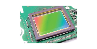
CMOS Image Sensor
Menangkap cahaya dengan presisi, mentransmisikan sinyal melalui struktur multilayer yang canggih.
CMOS (Complementary Metal-Oxide-Semiconductor) technology is prevalent in microprocessors, memory chips, and image sensors. CMOS image sensors contain pixel arrays with photodiodes and electronics for signal amplification and readout. Photodiodes generate electrical charge proportional to light intensity, converted into voltage, and read out from each pixel. Electromagnetic simulation tools like FEM and FDTD predict CMOS image sensor performance by modeling light absorption, photon-electron conversion, and charge transport, considering interactions between fields, thermal effects, and electrical behavior. This aids in thermal analysis, layout/material optimization for light sensitivity, and predicting electrical crosstalk impact on image quality.
Metamaterial
Metamaterial Fotonic Mengubah Revolusi Kontrol Optik dengan Nanostruktur
Metamaterials are artificial materials designed to exhibit unique properties not found in nature. They consist of periodic or aperiodic arrangements of subwavelength structures, enabling them to manipulate electromagnetic waves in unconventional ways. Simulation of transmission and reflection spectra is crucial for understanding how metamaterials interact with incident electromagnetic waves. This simulation helps identify resonance peaks, transmission bands, and reflection bands, providing valuable insights for designing metamaterial-based devices such as absorbers, filters, and antennas.
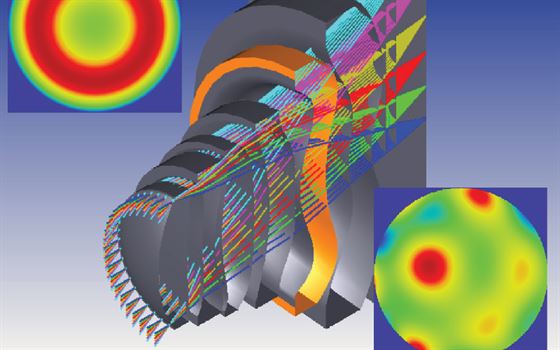
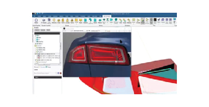
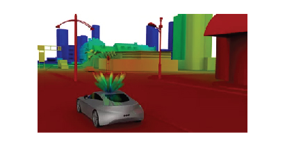
Automotive Optical Design Solutions
Memahami persyaratan dan merancang komponen optik kami sendiri menggunakan alat yang tersedia.
Automotive Optical Design Solutions encompass a range of technologies including LIDAR, Smart Lighting, HUD, ADAS, Rendering, and Lens Design. These solutions employ optical design and analysis to control light output, ensuring it meets specific requirements. The process involves conceptual studies, detailed design and development, result analysis, optimization, and final analysis. Optical engineers utilize optics to solve problems and design devices, requiring a deep understanding of optics and practical considerations such as technology, materials, and costs. Computers play a crucial role in their work, aiding in simulation, design, and analysis.
Photonic Crystal
Membongkar Struktur Pita dan Manipulasi Optik Melintasi Panduan Gelombang Planar, Persegi Panjang, dan Magneto-Optik
Photonic crystals are periodic nanostructures that control light flow akin to semiconductors with electrons. They consist of alternating high and low refractive index materials, creating a photonic band gap where light propagation is forbidden. Bandstructure analysis calculates the crystal’s band structure, revealing allowed and forbidden frequency ranges. It helps understand photonic band gaps and dispersion relations, characterizing properties like group velocity and phase velocity of guided modes.
Ansys Lumerical menawarkan alat-alat kuat untuk mensimulasikan pergerakan cahaya dalam gelombang pandu dan komponen fotonik, membantu insinyur mendesainnya secara akurat. Ini memperlihatkan bagaimana komponen-komponen ini berperilaku dan memungkinkan pengguna mengoptimalkannya untuk kinerja yang lebih baik. Produk ini menangani berbagai komponen fotonik dan aplikasi, memungkinkan pengembangan dan pengoptimalan desain yang tepat.
View Application
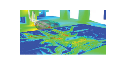
Optical and Lighting Technologies
Speos mensimulasikan kinerja optik dan mengevaluasi efek pencahayaan akhir berdasarkan kemampuan penglihatan manusia, yang dapat diterapkan dalam realitas virtual untuk pengalaman peninjauan yang sepenuhnya mendalam. Speos juga dapat mensimulasikan dan mengevaluasi sinyal mentah kamera dan lidar dalam lingkungan berkendara, memungkinkan tata letak sensor pada kendaraan dan mengevaluasi dampak versi desain terhadap persepsi sensor pada tahap awal.